

By Stefano Gallinaro,Analog Devices, Inc. & Imad Owaineh ,WATT&WELL
Analog Devices Isolated Gate Drivers, Power Supply Controllers, and Processors for Next-Generation Power Converters
The power converter market is and will be evolving fast, moving from simple performance/cost designs to broader and more sustainable innovation. New challenges are arising, such as the need to make smaller and more efficient power converters that can serve smaller servo drives or be integrated into distributed energy storage units. This also means having higher working voltage to manage higher power without increasing weight and dimension, like in solar string inverters and electric vehicle traction motors.
New high efficiency, ultrafast power converters based on wideband gap (WBG) semiconductors like silicon carbide (SiC) and gallium nitrite (GaN) MOSFETs are starting to expand in various innovative markets and applications—namely solar PV inverters, energy storage, and vehicle electrification (for example, chargers and traction motor inverters). To take all the advantages of the new power switch technologies, a complete ecosystem of ICs must be implemented in converter design, starting from the closest chip to the power switch, the gate driver. Requirements for isolated gate drivers are changing from past silicon IGBT drivers. For SiC and GaN MOSFETs, high CMTI >100 kV/μs, wide gate voltage swing, fast rise and fall times, and a very low propagation delay are needed. ADI’s ADuM4135 isolated gate driver has all the required technical features integrated in a 16-lead, wide-body SOIC package. Together with the ADSP-CM419F high end, mixed-signal control processor, they both can manage the high speed, complex multilevel control loops of the high density, SiC-/GaN-based, next-generation power converters.

Figure 1. Power converter market forecast for the year 2021.
The power converter market is growing with a CAGR of more than 6.5% and is expected to reach a value of 80 billion dollars by the year 2021. Today, traditional inverters and converters based on silicon IGBTs make up most of the market (>70%), primarily due to electrical motor drive applications in factory production lines and to the first generation of wind and solar inverters.
New technology improvements in power switches are bringing the third generation of SiC MOSFETs and the first and second generation of GaN MOSFETs to the market. After being restricted to some niche power applications for some time, WBG technologies are being quickly adopted in various applications, such as battery-based energy storage, electrical vehicle chargers, traction motors, and solar PV inverters. This expansion into newer markets has contributed to a rapid price reduction, which in turn has enabled entry into other markets where price had initially been a factor. Mass production has further decreased price and this will be continue to occur. The adoption of WBG semiconductors is a good example of a virtuous cycle in technology (and the economy at large).
The leading applications driving the usage of SiC/GaN power switches are solar PV inverters, electrical vehicle chargers, and energy storage converters. Here the added values of ultrafast, small, and efficient power switches are exploited to bring to the market extremely high switching frequencies and outstanding efficiency targets of more than 99%. To achieve all these results, designers are facing new challenges by cutting and reducing the weight and footprint (that is, increasing the power density) of the power converters.
Of course, solving these issues cannot be done all at once. Advances and innovations in all the related engineering processes are needed. One such example is the technological bottleneck related to the use of high voltage power electronics systems. Moving toward high voltage (HV) systems is an architectural choice, but for a long time it was hindered by some semiconductor technologies. Today, this has been remedied with the introduction of wideband gap semiconductors, which has made HV more feasible and worthy of consideration. The standard for solar string inverters is 1500 VDC, while 1000 VDC and soon 2000 VDC will be the standard for energy storage converters (battery based) and electric vehicle chargers.
Indeed, moving toward HV systems compatible with WBG semiconductors is interesting because of three reasons: firstly, high voltage implicates lower currents, which means that the total copper in the system will be reduced, and this is a reduction that has a direct impact on the cost reduction of the system. Secondly, wide gap technologies (enabled by HV) generate less resistive losses, which in turn present better efficiency and reduce the size and need for a cooling system. Finally, on a subsystem level, they will enable engineers to move from baseplate power module-based designs to discrete-based or lighter power module-based designs. This implies using compatible PCBs and smaller wires, instead of bus bars and heavier wires.
To conclude, high voltage systems are worthwhile if the reduction of weight and/or cost, or higher performances, are the core objectives of the design. The high breakdown voltage of 1.7 kV and 3.3 kV SiC MOSFETs is thus becoming a standard for 2nd level applications, while the 1.2 kV SiC MOSFETs are the mainstream power switches for next-generation 2nd and 3rd level applications.
From an engineering point of view, the advantages of SiC/GaN are considerable. To begin, the considerable dV/dt switching, inherent to WGB semiconductors, represents very little loss/switch. This makes a high switching frequency (50 kHz to 500 kHz for SiC, or >1 MHz for GaN) a very realistic possibility, which aids in helping to decrease the magnetics volume while increasing the power density. A reduction of more than 70% in the inductor value, size, and weight, together with reduced capacitors, can bring a final converter down to one fifth of the size and of weight of a traditional one. The savings in passive components and mechanics (including heat sink) are about 40%, with the added value being on the control electronics ICs.
Another huge advantage presented by these technologies is their tolerance to high thermal junction temperatures. Such a tolerance helps with increasing power density, while also limiting cooling problems.
Other characteristics of SiC/GaN switches that help reduce the losses are the absence of any recovery on the diodes (fewer losses on rectification), and the low Rds(on) (which generates less conduction) losses, in addition to their HV operation.
These advantages enable designing and implementing new and innovative power electronics topologies for new applications. SiC/GaN power switches are very beneficial in designing resonant circuits (such as LLC or PRC) or bridge topologies (phase-shift full bridge) or bridgeless power factor correction (PFC). That is due to their high switching frequencies, efficiency (thanks to zero voltage switching and zero current switching), and consequently high power density.
SiC-/GaN power transistors enable multilevel power conversion stages and full bidirectional working modes, where silicon IGBTs have limitations because of reverse operation.
The need of bidirectional working modes is becoming more and more mandatory for applications like energy storage, where the power flows to and from the batteries to the loads or to the grid. The possibility of designing high power converters with compact housing also allows a distributed energy storage system, where battery charging accuracy can be higher.
In order to achieve the many advantages obtained by SiC-/GaN-based designs, we should confront the various technical challenges associated with them. We can divide these challenges into three major categories: driving the switch, selecting the proper combo power supply, and controlling the power converter loops in a proper way.
Driving SiC MOSFETs, the engineer is confronted with new considerations such as the negative bias (needed for the gate driver) and the accuracy of the driving voltage (this is even more important for GaN). There is little tolerance for such imprecisions, and it could affect the whole system.
Analog Devices iCoupler® isolated gate drivers overcome the limitations of optocoupler- and high voltage-based gate drivers. Optocouplers are slow, power hungry, and difficult to integrate with other functions, and they degrade over time. By contrast, iCoupler digital isolators offer an alternative to optocouplers by combining high bandwidth on-chip transformers and fine scale CMOS circuitry that improve reliability, size, power, speed, timing accuracy, and ease of use for designers. iCoupler technology was created a decade ago to address the limitations of optocouplers. ADI’s digital isolators use low stress, thick film polyimide insulation to achieve thousands of volts of isolation that can be monolithically integrated with standard silicon ICs and can be fabricated in single-channel, multichannel, and bidirectional configurations: 20 μm to 30 μm of polyimide insulation withstand >5 kV rms.

Figure 2. iCoupler transformer coils on polyimide insulation.
The most representative ICs for ADI’s gate driver portfolio are the ADuM4135, the high end isolated gate driver for SiC MOSFETs and the ADuM4121, a fast, compact solution for high density SiC and GaN designs. Utilizing Analog Devices’ proven iCoupler technology, the ADuM4135 isolated gate driver offers a number of key benefits in high voltage and high switching speed applications. ADuM4135 is the best choice for driving SiC/GaN MOS due to a superior propagation delay of better than 50 ns with channel-to-channel matching of less than 5 ns, common-mode transient immunity (CMTI) of better than >100 kV/μs, and the capability to support lifetime working voltages of up to 1500 VDC in a single package.

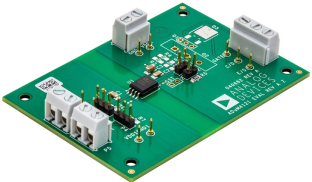
Figure 3. ADuM4135 evaluation board.

Figure 4. ADuM4135 block diagram.
The ADuM4135, in a 16-lead, wide-body SOIC package, includes a Miller clamp to provide robust SiC/GaN MOS or IGBT turn-off with a single-rail supply when the gate voltage drops below 2 V. Operation with unipolar or bipolar secondary supplies is possible. Integrated onto the ADuM4135 is a desaturation detection circuit that provides protection against high voltage, short-circuit switch operation. The desaturation protection contains noise reducing features, such as a 300 ns masking time after a switching event to mask voltage spikes caused by initial turn-on. An internal 500 µA current source allows for a low device count and the internal blanking switch allows for the addition of an external current source if more noise immunity is needed. The secondary UVLO is set to 11 V, with common IGBT threshold levels taken into consideration. Analog Devices iCoupler chip scale transformers also provide isolated communication of control information between the high voltage and low voltage domains of the chip. Information on the status of the chip can be read back from dedicated outputs. The control for resetting the device after a fault on the secondary is performed on the primary side of the device.
For more compact and simpler topologies (for example, GaN-based half bridges), the new ADuM4121 isolated gate driver is the solution. Also based on Analog Devices iCoupler digital isolation, it features a lowest-in-class propagation delay of 38 ns, which allows for the highest switching frequencies and the highest common-mode transient immunity of 150 kV/μs. ADuM4121 provides 5 kV rms isolation in a wide-body, 8-lead SOIC package.

Figure 5. ADuM4121 block diagram.

Figure 6. ADuM4121 evaluation board.
A critical aspect related to driving SiC/GaN switches is their operation under high voltage and high frequency conditions. Under such conditions, no capacitive or inductive parasitic elements should be tolerated at all. The designs are to be finely tuned and special care should be taken when routing the boards and defining their layout. This is a considerable, but necessary, challenge to avoid all EMI and noise issues. WBG semiconductor design requires high voltage and high frequency passive components (magnetics and capacitances). The challenges of sizing, designing, and manufacturing these devices should never be underestimated. Technology, however, keeps improving in these domains as well, and the possibilities provided by WGB semiconductors will inevitably make their procurement easier in the future.
As previously discussed, WBG semiconductors are especially effective for implementing high efficiency, high density topologies, and resonant topologies in particular. Yet these topologies are quite complex, and their control represents a challenge of its own. For example, the number of inputs needed to regulate a resonant topology (input voltage, input current, output voltage, etc.), combined with frequency modulation and phase modulation (on very high frequencies), does not make the engineer’s task any easier. The choice of digital components (DSP, ADC, etc.) is of utmost importance as well.
The system control units (generally a combination of MCUs, DSPs, or FPGAs) must have the capabilities of running multiple, high speed control loops in parallel and also be able to manage safety features. They have to provide redundancy and a large number of independent PWM signals, ADCs, and I/Os. Analog Devices’ ADSP-CM419F enables designers to have one mixed-signal dual-core processor managing parallel high power, high density, mixed-switch, multilevel power conversion systems.

Figure 7. ADSP-CM419F block diagram.
ADSP-CM419F is based on the ARM® Cortex®-M4 processor core, with a floating-point unit operating at frequencies up to 240 MHz, and it incorporates an ARM Cortex-M0 processor core operating at frequencies up to 100 MHz. This enables the integration of dual-core safety redundancy into a single chip. The main ARM Cortex-M4 processor integrates 160 kB of SRAM memory with ECC, 1 MB of flash memory with ECC, accelerators, and peripherals optimized for power converters’ control, like 24 independent PWM, and an analog module consisting of two 16-bit SAR type ADCs, one 14-bit on Cortex-M0 ADC, and one 12-bit DAC. The ADSP-CM419F operates from a single voltage supply, generating its own internal voltage supplies using internal voltage regulators and an external pass transistor. It comes in a 210-ball BGA package.

Figure 8. ADSP-CM419F evaluation board.
Analog Devices has engaged with WATT&WELL to work on a range of high end, SiC MOSFET-based power converters. The collaboration is starting with the design of high voltage, high current evaluation boards for ADI isolated gate drivers. High power specifications, such as 1200 V, 100 A, >250 kHz switching frequencies with a reliable and robust design, permit customers to completely evaluate the ADI set of ICs driving SiC and GaN MOSFETs.

Figure 9. Isolated gate driver board simplified block diagram.
In Figure 9, we can see the main components involved in the power switch drivers, from the LT3999 dc-to-dc transformer driver generating the positive gate voltage level to the REF19x (or LT1121x) high efficiency linear regulator making the negative gate voltage level, to the ADuM4135 isolated gate driver. The main controller is represented by the ADSP-CM419F processor, which can be embedded in the boards or connected with high frequency cabling and generate the PWM signals for the isolated gate drivers.
The challenge of providing a high performance driving circuit is not only having the best isolated gate driver in the market. Analog Devices’ uniqueness in the solution is the possibility of providing ready-to-go, complete system-level designs thanks to the integration of Analog Devices and Linear Technology (now a part of Analog Devices) devices. The combination of a dedicated power supply with stable and over-/under-shoot free voltage references is a must in applications running above 250 kHz. The PCB layout will initially be provided to strategic customers and then published on ADI’s website by the end of the year, together with schematics and user manuals.

Figure 10. Isolated gate driver board.
ADI and WATT&WELL are collaborating in this high end design that combines ADI know-how at silicon and at the system level, and WATT&WELL know-how for robust and reliable applications where high switching frequencies and power densities are coping with high temperature environments. The benefits of the collaboration permit Analog Devices to provide a fully workable solution to enable customers to implement new leading-edge designs in a short time-frame, which increases their competitiveness and reliability.
WATT&WELL’s mission is to be the premier power electronics design and manufacturing source for all those seeking innovation in O&G, automotive, aerospace, and industrial applications.
ADI enables our customers to interpret the world around us by intelligently bridging the physical and digital with unmatched technologies that sense, measure, and connect. We collaborate with our customers to accelerate the pace of innovation and create breakthrough solutions that are ahead of what’s possible.