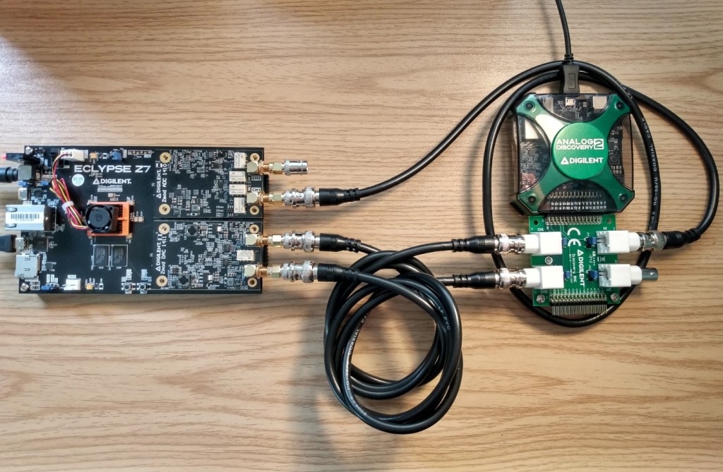
As more RF communications, test, software defined radio (SDR) and other similar applications press the technology further, Digilent, A National Instruments Company, has been hard at work to not only keep up the pace but also explore ways to influence the direction of this evolution. These trending applications employ high speed analog inputs and/or outputs where real-time signal processing is required, driving the need for higher precision and higher speed solutions.
Digilent’s latest FPGA board, the Eclypse Z7 Ecosystem is ideal for high-speed instrumentation, control, and measurement systems for edge-computing, medical, and communications applications.
The Eclypse Z7 ecosystem, available Excelpoint India, includes Eclypse Z7 Xilinx Zynq SoC Platform, Zmod ADC 1410 and Zmod DAC 1411. Zmods products are SYZYGY compliant expansion modules, a high-speed I/O expansion standard for FPGA boards intended to fit between the Pmod standard and FMC. The SYZYGY standard offers a much higher speed/bandwidth digital interface than Pmod but at a much smaller and lower-cost form-factor than FMC, enabling the user to configure a FPGA development board with the right I/O for their application.

Eclypse Z7
The Zmod ADC 1410 is equipped with Analog Devices AD9648, the dual channel, high speed, low power, 14-bit, 105MS/s Analog to Digital Converter (ADC). Driven by the SYZYGY carrier, the Zmod ADC can acquire two simultaneous signals (1MΩ, ±25V, single-ended, 14-bit, 100MS/s, 70MHz+ bandwidth). Analog inputs can be connected to a circuit using SMA cables.

Zmod ADC 1410
The Zmod DAC 1411 is equipped with Analog Devices AD9717 the dual channel, high speed, low power, 14-bit, 125MS/s Digital to Analog Converter (DAC). Driven by the SYZYGY carrier, the Zmod DAC can generate two simultaneous signals (50Ω, ±5V, single-ended, 14-bit, 100MS/s, 40MHz+ bandwidth). The analog outputs can be connected to a circuit using SMA cables.

Zmod DAC 1411
Signal Processing System Design
In this signal processing system, we will use the Digilent Analog Discovery 2, a USB multi-instrument, to generate analog signals and visualize output signals in the frequency domain and BNC Adapter to acquire signals from Zmods to Analog Discovery 2.

FPGA Based Signal Processing System
The simplified block diagram of the system implemented for this demo is shown below:

The analog signals from Analog Discovery 2 are converted to digital through the Zmod ADC 1410 and then passed on to the input of a digital low pass filter. The digital low pass filter is created by Xilinx FIR compiler 7.2 IP Core. The filter’s outputs are converted back to analog through the Zmod DAC 1411. These digital signals can be visualized through Zmod DAC 144 output channel 1. With this setup the frequency response of the filter can be correctly measured regardless of the gain setting of the Zmod DAC 1411. To correct the phase errors, there is a digital loopback by connecting Zmod ADC 1410 output channel directly to the Zmod DAC 1411 input channel 1.
The programmable logic of Zynq 7020 is used to
- Initializes the Zmod ADC 1410 hardware and synchronizes the incoming data in the user clock domain
- Create a digital low pass FIR filter by Xilinx FIR compiler 7.2 IP Core
- Initializes the Zmod DAC 1411 hardware and formats the output data according to the AD9717 DAC requirements
Operating the Signal Processing System
The Analog Discovery 2 Network Analyzer will be used to generate a sinusoidal signal (perturbation) on the Analog Discovery 2 Waveform Generator Channel 1. The Bode plot (see below) is obtained considering the loopback signal (Zmod DAC 411 CH2) as reference.

Bode Plot
The project details and source files are available at Digilent Wiki.


