

Source : Mouser Electronics
Electromobility still has quite a lot of challenges to overcome. Global environmental issues such as battery production, recycling, and power generation intertwine with individual and practical aspects like cost, battery capacity, and charging infrastructure. State-of-the-art semiconductor technology help solve at least some of the problems.
Silicon carbide (SiC) has been used as a semiconductor material for a long time. SiCwas first patented in 1906 as a radio detector diode and is commonly used in naval receiving technology. Similarly, the first commercial LEDs were based on SiC, and the material became renowned for creating yellow and blue LEDs. Because of difficulties in manufacturing, its application in power electronics happened only recently, over the past 20 years.
Eliminating crystal defects has turned out to be a major obstacle to SiC development. Edge dislocations, screw dislocations, triangular defects, and basal plane dislocations initially caused poor reverse blocking performance in devices made of SiC crystals. Apart from crystal quality, problems with the interface of SiC with silicon dioxide have hampered the development of SiC-based power MOSFETs and insulated-gate bipolar transistors. Only the still poorly understood nitridization has dramatically reduced the defects causing the interface problems. This cleared the way for JFETs, MOSFETs, and Schottky diodes from 2008 on. SiC, as a semiconductor material, has great advantages in speed, high temperature, and high voltage.
That’s exactly what’s needed in the harsh automotive environment. Electric cars use batteries with capacities of up to 100kWh, and the goal is to charge those in the least possible time. Charging an electric vehicle (EV) using public charging stations takes longer than refueling a fossil fuel vehicle. The speed at which a vehicle can recharge depends on the charging station’s charging speed and the vehicle’s capacity to receive a charge. Connecting a vehicle that can accommodate very fast charging to a charging station with a very high rate of charge can refill the vehicle’s battery to 80 percent in 15 minutes. Vehicles and charging stations with slower charging speeds can take as long as an hour to refill a battery to 80 percent. As with a mobile phone, the final 20 percent takes longer because the systems slow down to fill the battery safely and avoid damaging it.
Alternating current (AC) charging stations connect the vehicle’s onboard charging circuitry directly to the AC Supply. AC Level 1 connects directly to a 120V residential outlet, capable of supplying 12A to 16A (1.4kW to 1.92kW) depending on the capacity of a dedicated circuit. AC Level 2 utilizes 240V residential or 208V commercial power to supply between 6A and 80A (1.4kW to 19.2 kW).
In direct current (DC) fast charging, grid power is passed through an AC/DC inverter before reaching the vehicle’s battery, bypassing the onboard charging circuitry. DC Level 1 supplies a maximum of 80kW at 50V-1000V, and DC Level 2 delivers a maximum of 400kW at 50V-1000V. A standard for larger commercial vehicles is under development, with a theoretical maximum power of 4.5MW.
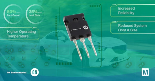
Diodes, MOSFETs, and drivers are the major components of such high-power charging circuitry. With their increased switching speed and decreased power losses, the Wide Bandgap SiC Device Portfolio from ON Semiconductor delivers the right components for every part of modern solutions. The need for protection circuits is reduced by implementing galvanically isolated High-Current Gate Drivers.
On Semiconductor’s NCx57200 is a high-voltage gate driver with one non-isolated low-side gate driver and one galvanic isolated high- or low-side gate driver. The devices can directly drive two insulated-gate bipolar transistors (IGBTs) in a half-bridge configuration. The galvanic isolation for the high-side gate driver ensures reliable switching in high-power applications for IGBTs that operate up to 800V at high dv/dt. The optimized output stages provide a means of reducing IGBT losses. The features include two independent inputs with deadtime and interlock, accurate asymmetric undervoltage-lockouts (UVLOs), and short and matched propagation delays. With a bandwidth range of 270kHz to 3MHz, operational amplifiers with typical IQ of 17µA to 405µA allow for safe sensing circuits in the charging networks.
However, circuit protection is still necessary. The AEC−Q100-qualified: NCID9211 Dual-Channel Digital Isolator achieves high insulation and high noise immunity, characterized by high common-mode rejection (100KV/s minimum) and power supply rejection. As ON Semiconductor’s Protection & Small Signal Discretes demonstrate, fuses and filters take care of the rest.
Conclusion
ON Semiconductor has put extra effort into solving some of the challenges related to SiC previously mentioned, such as crystal defects or gate oxide reliability. By adding additional quality control steps in the manufacturing process like wafer screening or burn-in tests, the intrinsic crystal defects in SiC can be better filtered. Moreover, the reinforced gate oxide in the SiC MOSFETs enables dynamic negative gate bias without a drift in RDS(ON) or Vth. The outcome is reliable SiC devices ready to be used in the most challenging applications such as EV charging.
To learn more, visit www.mouser.com