
Current challenges and possible solutions in the charger segment
By Tim Hu, Senior Marketing Manager, Infineon Technologies
The growing popularity of mobile electronic devices has led to a wide range of different charger/adapter types. In order to reduce electronic waste and to improve user experience, associations, governors and the European Union as well has initiated charger unification to establish a common charger standard for all mobile device manufacturers (mainly in Europe). The USB Type-C connector and the USB-PD standard undoubtedly can support these market trends by on the one hand providing up to 100 W charging power with a unified connector, on the other unification by the USB-PD single charging standard.
In addition to the above-mentioned trigger, there is a market trend in charger designs too that pushes towards smaller form factors and increased charging power to fulfill requirements such as larger battery capacities and shorter charging times. More power in small form factors is equivalent to an increase in power density, thus efficient power converters have to catch up with the market trend.
Current challenges in the charger market
As a typical end-consumer oriented mass product, chargers are preferably low on cost while competitive in performance. This poses challenges to design engineers. Benefiting from their long experience in switching power designs, engineers realized that the most common power topology for chargers are flyback converters. It is because this flyback topology is relatively easy to implement hence decreases design efforts and time-to-market, and importantly, this is the only magnetic component topology that can bring cost advantages too. However, it has a disadvantage: the common converter efficiency limited the possibly achievable power density which lately has become a very important differentiating factor. In order to achieve higher power density, designers can consider several options. They can either adapt zero-voltage-switching (ZVS) control methods to reduce switching losses or use high-performance power MOSFETs in compact packages (i.e., ThinPAK 8×8) to shrink the charger size or increase operating frequency to reduce for example transformer-, electrolytic capacitor- as well as EMI filter size. Utilizing these approaches leads to having >15 W/in³ chargers available in the market today.
Infineon offers a wide variety of high-quality high- and low-voltage power MOSFETs as well as digital soft-switching controllers to enable design USB-PD design engineers to meet their design targets in terms of power efficiency and reliability.

Controller requirements and recommendation
Knowing that a standard flyback converter only allows for a certain, very low power density, Infineon has investigated and evaluated lots of suitable topologies and control schemes suitable for high-density USB-PD charger designs to overcome this technology barrier. Infineon´s XDP™ digital controller family embeds a microprocessor core surrounded by all digital and analog circuits needed to realize a power supply with only a few external components.
The digital-based XDPS21071 is the first flyback controller in the industry with ZVS on the primary side to achieve high efficiency with simplified circuitry and economical switches resulting in lower BOM cost. By negative magnetization, the forced-frequency-resonant (FFR) switching scheme reduces the losses associated with today’s valley-switching type of controllers without sacrificing the design simplicity of fixed-frequency switching schemes. Besides, thanks to its digital control, many parameters are adjustable to simplify BOM. It also provides great flexibility, allows for tailor-making designs based on different system specifications. The FFR control method helps achieve efficiency beyond 90 percent at balanced BOM costs, the high volume shipment had already proven that FFR is a strong candidate to help improve USB-PD design performance.
In case of even higher efficiency targets, an asymmetric flyback topology is recommended (for an efficiency level of 93 percent). This is also known as a hybrid flyback scheme because this converter operates in mixed flyback/forward mode. The hybrid topology features ZVS in the primary-side half-bridge by utilizing the magnetization current, and zero-current switching (ZCS) in the synchronous rectification switch, laying the foundation for the highest conversion efficiency. This converter[ This digital-based hybrid flyback controller will be soon available from Infineon.] demonstrates 93.8 percent efficiency under worst-case conditions and a peak efficiency of 95 percent, while the uncased power density is at around 27 W/in³. (In reality, the power density of the cased converter will not be higher than 22 W/in³ to avoid a thermal runaway).
Power switch requirements and recommendation
For highly efficient power management required in contemporary charger designs, high-performance power switches are needed.
The CoolMOS™ product family is a proven high-performance high-voltage superjunction MOSFET series that physically breaks the silicon limit to achieve ever lower RDS(ON) x Area. The latest 700 V P7 and 600 V PFD7 series are specifically targeting the charger market with their cost-competitiveness, low switching losses, great thermal behavior, and allow for high-speed switching. The integrated ESD ruggedness is up to the HBM class 2 level, which enables increased assembly yields, and leads to less production-related failures and consequently saves manufacturing costs. In addition, the available several package variants can further support USB-PD charger competitiveness, for example, the cost-effective SOT-223 package is a perfect drop-in replacement for DPAK at a lower cost. Figure 2 shows a ThinPAK package characterized by very low source inductance, separate driver source connection for clean gate signals, and highly improved commutation loop (MOSFET, diode, cap) that leads to lowest stray inductances resulting in lower VDS overshoots. As a result, the ThinPAK package enables faster and more efficient switching of power MOSFETs and is also easier to handle in terms of switching behavior and EMI.

To push the power density to even higher levels, the use of GaN HEMTs (i.e., CoolGaN™) is favorable. They enable increased converter efficiency, and thus to move away from the thermal limit. One of the key advantages of GaN-based devices is given by the greatly reduced QOSS charge which enables ZVS with lower magnetization current. This way, the conduction losses in the switches, as well as in the transformer, can be reduced. Furthermore, due to the lower gate charge, the gate-driving losses are reduced. Last but not least, the losses associated with the charging/discharging of COSS capacitance of the switches during ZVS are also lower in GaN HEMTs than in superjunction MOSFETs.
Out of the silicon-based product offering of Infineon, the OptiMOS™ PD portfolio is also well-suited for USB-PD chargers as synchronous rectification and loading switches. It is because the family features MOSFETs with low on-state resistance (RDS(ON)), less switching losses as well as low gate-, output- and reverse recovery charges. This reduction in the total losses results in an excellent price/performance ratio contributing to a decrease in the system BOM cost. Logic-level availability enables parts to be fully driven from 4.5 V or directly from microcontrollers. This results in lower part count within the application, while the PQFN 3.3 x 3.3 and SuperSO8 packages can help shrink USB-PD charger form factors.
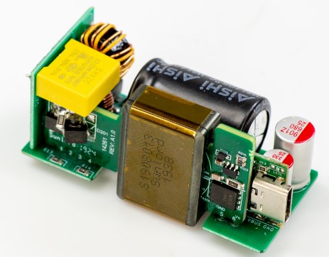
A USB-PD reference design from Infineon
Infineon recently has released the ready-to-use 45 W 20 W/in3 (50 CC) USB-PD digital reference design (Figure 3). This silicon-based solution offers a robust, high power density, low-cost, and scalable platform for USB-PD designs. A planar transformer and SMD packages are used to increase production capability and enable ultrathin designs.

Summary
The USB-PD standard gains more traction as the need for unification has become more dominant in the charger market. This triggers R&D efforts and advancements in the semiconductor market too. There are already several solutions available that meet the USB-PD design requirements.
Infineon, one of the world-leading power semiconductor companies, offers a comprehensive portfolio to enable high-density USB-PD charger designs. The digital-based XDP™ controller brings the new control methods for ZVS/ZCS operation to enhance flyback converters, the tailor-made HV superjunction CoolMOS™ MOSFETs and the low-voltage OptiMOS™ devices provide cost-effective solutions that increase market competitiveness, while the GaN-based integrated-power-stage devices can further push power density in USB-PD chargers to a higher level, while the introduced 45 W reference design makes it easy to achieve 20 W/in³ density USB-PD charger for mobile electronic devices.
For more information, please visit the www.infineon.com/usb-pd webpage or scan the QR code.