
Introduction
This article discusses the history and design challenges for designing a resistance temperature detector (RTD)-based temperature measurement system. It also covers RTD selection and configuration trade-offs. Finally, it details RTD system optimization and evaluation.
Why Is RTD Temperature Measurement Important?
Temperature measurement plays an important role in many different end applications such as industrial automation, instrumentation, CbM, and medical equipment. Whether monitoring environmental conditions or correcting system drift performance, high accuracy and precision are very important. There are several types of temperature sensors that can be used such as thermocouples, resistance temperature detectors (RTDs), electronic band gap sensors, and thermistors. The temperature sensor selected along with the design depends on the temperature range being measured and the accuracy required. For temperatures in the range of –200°C to +850°C, RTDs provide an excellent combination of high accuracy and good stability.
What Are the Main Temperature Measurement Challenges?
Challenges include
- Current and voltage selection. An RTD sensor is a passive device and does not produce an electrical output on its own. Excitation current or voltage is used to measure the resistance of the sensor by passing a small electrical current through the sensor to generate a voltage. How do I select the current/voltage?
- Is a 2-wire, 3-wire, or 4-wire the best choice for my design?
- How should the RTD signal be conditioned?
- How do I adjust the above variables so that the converter or other building blocks are used within their specification?
- Connecting multiple RTDs in a system—how are the sensors connected? Can some blocks be shared among the different sensors? And what is the impact to the overall system performance?
- What is the expected error for my design?
RTD Selection Guide
RTD Overview
For an RTD, the resistance of the sensor varies as a function of temperature in a precisely defined manner. The most widely used RTDs are platinum Pt100 and Pt1000, which are available in 2-wire, 3-wire, and 4-wire configurations. Other RTD types are made from nickel and copper.
Table 1. Common RTD Types
| RTD Type | Materials | Range |
| Pt100, Pt1000 | Platinum (numeric is resistance at 0°C) | –200°C to +850°C |
| Pt200, Pt500 | Platinum (numeric is resistance at 0°C) | –200°C to +850°C |
| Cu10, Cu100 | Copper (numeric is resistance at 0°C) | –100°C to +260°C |
| Ni120 | Nickel (numeric is resistance at 0°C) | –80°C to +260°C |
The most common Pt100 RTDs can take two different shapes: wire wound and thin film. Each type is built to several standardized curves and tolerances. The most common standardized curve is the DIN curve. DIN stands for “Deutsches Institut für Normung,” which means “German institute for standardization.” The curve defines the resistance vs. temperature characteristics of a platinum 100 Ω sensor, the standardized tolerances, and the operating temperature range. This defines the accuracy of the RTD starting with a base resistance of 100 Ω at a temperature of 0°C. There are different standard tolerance classes for DIN RTDs. These tolerances are shown in Table 2, and they also apply to Pt1000 RTDs that are useful in low power applications.
Table 2. RTD Accuracy—Class A, Class B, 1/3 DIN
| Sensor Type | DIN Class | Tolerance @ 0°C | Tolerance @ 50°C | Tolerance @ 100°C |
| Pt100 RTD Thin Film | Class B | ±0.30°C | ±0.55°C | ±0.80°C |
| Pt100 RTD Thin Film | Class A | ±0.15°C | ±0.25°C | ±0.35°C |
| Pt100 RTD Wire Wound/ Thin Film | 1/3 Class B | ±0.1°C | ±0.18°C | ±0.27°C |
Both the RTD itself and its accuracy must be considered when selecting the RTD sensor. The temperature range varies with element type, and the accuracy denoted at calibration temperature (usually at 0°C) varies with temperature. Thus, it is important to define the temperature range being measured and take into consideration that any temperature below or above the calibration temperature will have a wider tolerance and lower accuracy.
RTDs are categorized by their nominal resistance at 0°C. A Pt100 sensor has a temperature coefficient of approximately 0.385 Ω/°C and a Pt1000 has a temperature coefficient that is a factor of 10 greater than the Pt100. Many system designers use these coefficients to get an approximate resistance to temperature translation, but the Callendar-Van Dusen equations provide a more accurate translation.
The equation for temperature t ≤ 0°C is

The equation for temperature t ≥ 0°C is

where:
- t is the RTD temperature (°C)
- RRTD(t) is the RTD resistance at temperature (t)
- R0 is the RTD resistance at 0°C (in this case, R0 = 100 Ω) A = 3.9083 × 10⁻³
- B = −5.775 × 10⁻⁷
- C = −4.183 × 10⁻¹²
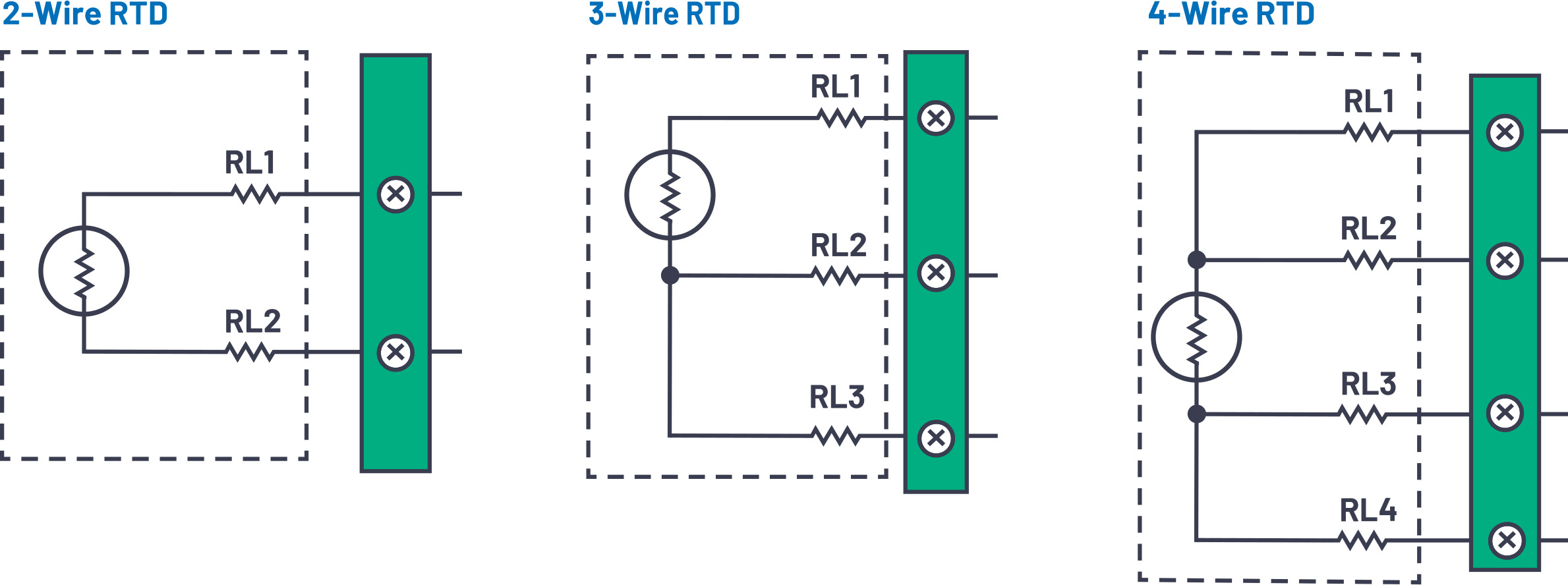
RTD Wiring Configurations
Another sensor parameter that needs to be considered when selecting an RTD is its wiring configuration, which will affect system accuracy. There are three different RTD wiring configurations available in the market wherein each configuration has advantages and disadvantages over one another and may require different techniques to reduce the measurement error.
A 2-wire configuration is the simplest but the least accurate configuration due to errors in lead-wire resistance and its variation with temperature contributing a significant measurement error. Thus, this configuration is only useful in applications where lead wires are short or when using a high resistance sensor (for example, Pt1000), both of which minimize lead resistance effects on the accuracy.
3-wire is the most used configuration because of the advantage of using three pins, which are useful in designs where the connector size is minimized (three connection terminals required vs. the 4-wire terminal for a 4-wire RTD). 3-wire also has significant accuracy improvement over the 2-wire configuration. The lead-wire resistance error in 3-wire can be compensated using different calibration techniques that will be later covered in this article.
4-wire is the most expensive but the most accurate configuration. In this configuration, the errors due to lead-wire resistance, along with temperature variation effects, are removed. Therefore, a 4-wire configuration results in the best performance.
RTD Configuration Circuit
A high precision and accurate RTD sensor measurement requires precise signal conditioning, analog-to-digital conversion, linearization, and calibration. The typical design of an RTD measurement system consists of the different stages as shown in Figure 2. Although the signal chain looks simple and straightforward, there are several complex factors involved and designers must consider complex component selection, connection diagram, error analysis, and other analog signal conditioning challenges that impact overall system board size and the cost of the bill of materials (BOM) due to the higher number of contributing blocks. On the brighter side, there are plenty of integrated solutions available in ADI’s portfolio. This complete system solution helps designers to simplify their designs while reducing the board size, time to market, and the cost of the overall RTD measurement system.

Figure 1. RTD wiring configurations

Figure 2. Typical RTD measurement signal chain block.
The three RTD wiring configurations have different wiring techniques needed to interface or connect an RTD to an ADC, along with the other external components, and requirements from the ADC, such as excitation current and a flexible mux. This section covers a deeper understanding and focus on each RTD configuration circuit design and considerations.
Sigma-Delta ADCs
Sigma-delta (Σ-Δ) ADCs offer multiple benefits when designing RTD systems. Firstly, as sigma-delta ADCs oversample the analog input, external filtering is minimized, with a simple RC filter being the only requirement. They offer flexibility in terms of choice of filter type and choice of output data rate. The inbuilt digital filtering can be used to reject any interference from the mains power supply in mains operated designs. 24-bit, high resolution ADCs such as the AD7124-4/AD7124-8 have a peak-to-peak resolution of 21.7 bits maximum. Other benefits are
- Wide common-mode range for the analog inputs
- Wide common-mode range for the reference inputs
- Ability to support ratiometric configurations
- Buffered reference and analog inputs
Some sigma-delta ADCs are highly integrated and include
- A programmable gain amplifier (PGA)
- Excitation currents
- Reference/analog input buffers
- Calibration functions
They simplify the RTD design significantly along with reducing the BOM, system cost, board space, and time to market.
For this article, the AD7124-4/AD7124-8 are used as the ADC. These are low noise, low current precision ADCs with an integrated PGA, excitation currents, analog input, and reference buffers.
Ratiometric Measurement
A ratiometric configuration is a suitable and cost-effective solution for systems that use resistive sensors such as RTDs or thermistors. With a ratiometric approach, the reference and sensor voltages are derived from the same excitation source. Therefore, the excitation source does not need to be accurate. Figure 3 shows an example of a ratiometric configuration in a 4-wire RTD application. A constant excitation current supplies the RTD and a precision resistor, RREF, with the voltage generated across RREF being the reference voltage for the RTD measurement. Any variation of the excitation current does not affect the accuracy of the measurement. Therefore, using a ratiometric approach allows a noisier, less stable excitation current to be used. An excitation current is preferred over voltage excitation due to its better noise immunity. The major factors to consider when selecting an excitation source value are discussed later in this article.

Figure 3. 4-wire RTD ratiometric measurement.
Shared IOUT/AIN Pin
Many RTD system designers use sigma-delta ADCs with integrated mux and excitation currents that allow multiple channel measurements and flexible routing of the excitation currents to each sensor. An ADC such as the AD7124 allows a single pin to operate simultaneously as an excitation current and an analog input pin (see Figure 4). Sharing pins between IOUT and AIN will only require two pins per 3-wire RTD sensor, which increases the channel count. However, in this configuration, a large value of the resistor R in the antialiasing or electromagnetic interference (EMI) filtering can add errors to the RTD resistance value as R is in series with the RTD—thus, limited R values can be used. That’s why it is usually recommended to have a dedicated pin for each excitation current source to avoid possible errors across RTD measurements.

Figure 4. 3-wire RTD with a shared IOUT/AIN pin.
4-Wire RTD Connection Diagram
A 4-wire RTD configuration offers the best performance. The only issue that system designers face is the cost of the sensor itself and the size of the 4-pin connector compared to the other two configurations. In this configuration, the errors due to the lead wires are inherently removed by the return wires. A 4-wire configuration uses Kelvin sensing with two wires to carry the excitation current to and from the RTD, while the remaining two wires sense the current across the RTD element itself. Errors due to lead resistance are inherently removed. A 4-wire configuration only requires one excitation current IOUT, as shown in Figure 5. Three analog pins from the ADC are used to implement a single 4-wire RTD configuration: one pin for excitation current, IOUT, and two pins as a fully differential input channel (AINP and AINM) used for sensing the voltage across the RTD.
When the design uses multiple 4-wire RTDs, a single excitation current source can be used with the excitation current being directed to the different RTDs in the system. By placing the reference resistor on the low side of the RTD, a single reference resistor can support all the RTD measurements; that is, the reference resistor is shared by all RTDs. Note that the reference resistor can be placed on the high side or low side if the ADC’s reference input has wide common-mode range. So, for a single 4-wire RTD, either the reference resistor on the high side or low side can be used. However, when using multiple 4-wire RTDs in a system, placing the reference resistor on the low side is advantageous as one reference resistor can be shared by all RTDs. Note that some ADCs include reference buffers. These buffers may require some headroom, so a headroom resistor is then required if the buffer is enabled. Enabling the buffer means that more robust filtering can be connected to the reference pins without causing errors such as gain errors within the ADC.
2-Wire RTD Connection Diagram
The 2-wire RTD configuration is the simplest configuration and is shown in Figure 6. For the 2-wire configuration, only one excitation current source is required. Thus, three analog pins from the ADC are used to implement a single 2-wire RTD configuration: one pin for excitation current, IOUT, and two pins as a fully differential input channel (AINP and AINM) used for sensing the voltage across the RTD. When the design uses multiple 2-wire RTDs, a single excitation current source can be used with the excitation current being directed to the different RTDs in the system. By placing the reference resistor in the low side of the RTD as per the 4-wire configuration, a single reference resistor can support all the RTD measurements; that is, the reference resistor is shared by all RTDs.
The 2-wire configuration is the least accurate of the three different wiring configurations since the actual resistance at the point of measurement includes both the resistances of the sensor and the lead wires RL1 and RL2, thus increasing the voltage measurement across the ADC. If the sensor is remote and the system uses a very long wire, then the errors will be significant. For example, a 25-foot length of a 24 AWG copper wire will have an equivalent resistance of 0.026 Ω/foot (0.08 Ω/meter) × 2 × 25 foot is to 1.3 Ω. Therefore, 1.3 Ω wire resistance produces an error of (1.3/0.385) = 3.38°C (approximately) due to wire resistance. The wire resistance also changes with temperature, which adds additional error.

Figure 5. Single and multiple 4-wire RTD analog input configuration measurements.
3-Wire RTD Connection Diagram
The significant error due to lead-wire resistances of the 2-wire RTD configuration can be significantly improved by using a 3-wire RTD configuration. In this article, we use a second excitation current (shown in Figure 7) to cancel the lead-wire resistance errors produced by RL1 and RL2. Thus, four analog pins from the ADC are used to implement a single 3-wire RTD configuration: two pins for excitation currents (IOUT0 and IOUT1) and two pins as a fully differential input channel (AINP and AINM) used for sensing the voltage across the RTD.

Figure 6. Single and multiple 2-wire RTD analog input configuration measurement.

Figure 7. Single and multiple 3-wire RTD analog input configuration measurement.
There are two ways to configure a 3-wire RTD circuit. Method 1 places the reference resistor on the top side so the first excitation current IOUT0 flows to RREF, RL1 then to RTD, and the second current flows through the RL2 lead resistance and develops a voltage that cancels the voltage dropped across the RL1 lead resistance. So, well matched excitation currents null the error due to the lead resistance completely. If the excitation currents have some mismatch, the impact of the mismatch is minimized using this configuration. The same current flows to the RTD and RREF; thus, any mismatch between the two IOUTs affects the lead resistance calculation only. This configuration is useful when measuring a single RTD.
When measuring multiple 3-wire RTDs, a reference resistor on the bottom side is recommended (Method 2) so only a single reference resistor can be used, which minimizes the overall cost. However, in this configuration, one current flows through the RTD while both currents flow through the reference resistor. So, any mismatch in IOUT can affect the value of the reference voltage along with the lead resistance cancellation. When excitation current mismatch is present, this configuration will have greater error than Method 1. There are two possible ways to calibrate the mismatch and mismatch drift between IOUT, hence improving the accuracy of the second configuration. First is calibrating by chopping (swapping) the excitation currents, performing a measurement on each phase, and then averaging the two measurements. Another solution is to measure the actual excitation currents themselves and then use the calculated mismatch to compensate for the mismatch in the microcontroller. More details regarding these calibrations are discussed in CN0383.
RTD System Optimization
Looking at system designer issues, there are different challenges involved in designing and optimizing RTD application solutions. Challenge one is the sensor selection and connection diagram that were discussed in the previous sections. Challenge two is the measurement configuration, which includes the ADC configuration, setting the excitation current, setting the gain, and selecting the external components while ensuring system optimization and operating within the ADC specification. And lastly, the most critical issue is how to achieve the target performance and what are the error sources that contribute to the overall system error.
Luckily, there is a new RTD_Configurator_and_Error_Budget_Calculator that offers a hands-on solution in designing and optimizing RTD measurement systems from concept to prototyping.
The tool
- Enables the understanding of the correct configuration, wiring, and circuit diagram
- Assists in the understanding of the different error sources and allows design optimization
The tool is designed around the AD7124-4/AD7124-8. It allows the customer to adjust settings such as excitation current, gain, and external components. It indicates out-of-bound conditions to ensure that the final solution is within the specifications of the ADC.

Figure 8. RTD configurator.
Selection of Excitation Current, Gain, and External Components
Ideally, we tend to select higher magnitudes of excitation current to generate a much higher output voltage and maximize the ADC input range. However, since the sensor is resistive, the designer must also ensure the power dissipation or self-heating effects of a large value of excitation current will not affect the measurement results. A system designer may select a high excitation current. However, to minimize self-heating, the excitation current needs to be turned off between measurements. The designer needs to consider the timing implications for the system. An alternative approach is to select a lower excitation current that minimizes self-heating. Timing is now minimized, but the designer needs to determine if system performance is affected. All scenarios can be tested via the RTD_Configurator_and_Error_Budget_Calculator. The tool allows the user to balance the selection of excitation current, gain, and external components to ensure that the analog input voltage is being optimized along with tuning the ADC gain and speed to give better resolution and better system performance, which means lower noise and lower offset error.
To understand the resulting filter profile or to get a deeper understanding of the timing of the conversions, the VirtualEval online tool provides this detail.
The ADC input and reference inputs of a sigma-delta ADC are both continuously sampled by a switched capacitor front end. For the RTD systems being discussed, the reference input is also driven by an external reference resistor. An external RC filter is recommended on the analog input of a sigma-delta ADC for antialiasing purposes. For EMC purposes, a system designer may use large R and C values both on the analog input and the reference input. Large RC values can cause gain errors in measurements as the front-end circuitry does not have sufficient time to settle between sampling instants. Buffering the analog and reference inputs prevents these gain errors and allows unlimited R and C values to be used.
For the AD7124-4/AD7124-8, when using an internal gain greater than 1, the analog input buffers are automatically enabled and since the PGA is placed in front of the input buffers, as the PGA is rail to rail, the analog input is also rail to rail. However, in the case of the reference buffers or when using the ADC at a gain of 1 with analog input buffers enabled, it is necessary to ensure that the headroom required for correct operation is met.
Signals from Pt100s are low level. They are in the order of hundreds of mV. For optimum performance, an ADC with wide dynamic range can be used. Alternatively, a gain stage can be used to amplify the signal before it is applied to the ADC. The AD7124-4/AD7124-8 support gains from 1 to 128, thus allowing an optimized design for a wide range of excitation currents. The multiple allowed options of PGA gain allow the designer to trade off excitation current value vs. gain, external components, and performance. The RTD configurator tool indicates whether the new excitation current values can be used with the selected RTD sensor. Suitable values for the precision reference resistor and the reference headroom resistor are also suggested. Note that the tool ensures the ADC is used within specification—it displays possible gains that will support the configuration. The AD7124 excitation currents have an output compliance; that is, the voltage on the pin providing the excitation current needs some headroom from AVDD. The tool will also ensure that this compliance specification is met.
The RTD tool allows the system designer to guarantee a system that is within the operating limits of the ADC and the RTD sensor. The accuracy of the external components such as the reference resistor and its contribution to the system error will be discussed later.
Filtering Options (Analog and Digital 50 Hz/60 Hz Rejection)
As discussed earlier, an antialiasing filter is recommended with sigma-delta converters. As the embedded filter is digital, the frequency response is reflected around the sampling frequency. Antialiasing filtering is required to adequately attenuate any interference at the modulator frequency and at any multiples of this frequency. Since sigma-delta converters oversample the analog input, the design of the antialiasing filter is greatly simplified and a simple single-pole RC filter is all that is required.
When the final system is used in the field, dealing with noise or interference from the environment in which the system is operating can be quite challenging, especially in application spaces such as industrial automation, instrumentation, process control, or power control, wherein being tolerant to noise and at the same time not being noisy to your neighboring components is required. Noise, transients, or other interference sources can impact the system accuracy and resolution. Interferences can also occur when systems are powered from the mains supply. Main power supply frequencies are generated at 50 Hz and its multiples in Europe, and 60 Hz and its multiples in the U.S. Thus, when designing an RTD system, a filtering circuit with 50 Hz/60 Hz rejection must be considered. Many system designers want to design a universal system that rejects both 50 Hz and 60 Hz simultaneously.
Most of the lower bandwidth ADCs, including AD7124-4/AD7124-8, offer a variety of digital filtering options that can be programmed to set notches at 50 Hz/60 Hz. The filter option selected has an effect on the output data rate, settling time, and the 50 Hz and 60 Hz rejection. When multiple channels are enabled, a settling time is required to generate a conversion every time the channel is switched; thus, selecting a filter type with longer settling time (that is, sinc4 or sinc3) will lower the overall throughput rate. In this case, a postfilter or FIR filter is useful to provide reasonable simultaneous 50 Hz/60 Hz rejection at lower settling times and thus increasing the throughput rate.
Power Consideration
The current consumption or power budget allocation of the system is highly dependent on the end application. The AD7124-4/AD7124-8 contain three power modes that allow trade-off between performance, speed, and power. For any portable or remote application, low power components and configurations must be used, and for some industrial automation applications, the complete system is powered from the 4 mA to 20 mA loop so that a current budget of only 4 mA maximum is allowed. For this type of application, the devices can be programmed in mid or low power mode. The speed is much lower, but the ADC still gives high performance. If the application is process control, which is powered from the mains supply, a much higher current consumption is allowed, so the device can be programmed in full power mode and this system can achieve a much higher output data rate and increased performance.
Error Sources and Calibration Options
After knowing the required system configuration, the next step is to estimate the errors associated with the ADC and the system errors. These help system designers to understand if the front end and ADC configuration will meet the overall target accuracy and performance. The RTD_Configurator_and_Error_Budget_Calculator allows the user to modify the system configuration for optimum performance. For example, Figure 9 shows a summary of all the errors. The system error pie chart indicates that the external reference resistor’s initial accuracy and its temperature coefficient are the main error contributors to the overall system error. Thus, it is important to consider using an external reference resistor with higher accuracy and a better temperature coefficient.
The error due to the ADC is not the most significant error contributor to the overall system error. However, the error contribution from the ADC can be reduced further using the AD7124-4/AD7124-8’s internal calibration modes. An internal calibration is recommended upon power-up or software initialization to remove the ADC gain and offset errors. Please note that these calibrations will not remove errors created by the external circuitry. However, the ADC can also support system calibrations so that the system offset and gain error can be minimized, but this may add additional cost and may not be required for most applications.
Fault Detection
For any harsh environment or for applications where safety is a priority, diagnostics are becoming part of the industry requirements. The embedded diagnostics in the AD7124-4/AD7124-8 reduce the need for external components to implement diagnostics, resulting in a smaller, simplified time and cost savings solution. Diagnostics include
- Checks of the voltage level on the analog pins to ensure it is within the specified operating range
- A cyclic redundancy check (CRC) on the serial peripheral interface (SPI) bus
- A CRC on the memory map
- Signal chain checks
These diagnostics lead to a more robust solution. The failure modes, effects, and diagnostic analysis (FMEDA) of a typical 3-wire RTD application have shown a safe failure fraction (SFF) greater than 90% according to IEC 61508.
RTD System Evaluation
Figure 10 shows some measured data from note CN0383. This measured data was captured with the AD7124-4/AD7124-8 evaluation board, which includes demo modes for 2-, 3-, and 4-wire RTDs, and calculated the corresponding degree Celsius value. The results show that a 2-wire RTD implementation gives an error closer to the lower limit of the error boundary, while the 3-wire or 4-wire RTD implementation has an overall error that is well within the allowed limit. The higher error in the 2-wire measurement is due to the lead resistance errors described earlier.

Figure 9. RTD error sources calculator
What these examples show is that following the above RTD guidelines will lead to a high accuracy, high performance design when used in conjunction with ADI’s lower bandwidth sigma-delta ADCs such as the AD7124-4/AD7124-8. The circuit note (CN0383) will also serve as a reference design that helps the system designer get to prototyping quickly. The evaluation board allows the user to evaluate the system performance wherein each of the sample configuration demo modes can be used. Going forward, firmware for the different RTD configurations can be easily developed using ADI generated sample code available from the AD7124-4/AD7124-8 product pages.
ADCs, which use a sigma-delta architecture such as from the AD7124-4/AD7124-8, are suitable for RTD measurement applications since they address concerns such as 50 Hz/60 Hz rejection, as well as wide common-mode range on the analog and possibly the reference inputs. They are also highly integrated, containing all the functions needed for an RTD system design. In addition, they provide enhanced features such as calibration capability and embedded diagnostics. This level of integration, along with the complete system collateral or ecosystem will simplify the overall system design, cost, and design cycle from concept to prototyping.
To ease the system designers’ journey, the RTD_Configurator_and_Error_Budget_Calculator tool along with the online tool VirtualEval, the evaluation board hardware and software, and CN0383 can be used to address the different challenges, such as connectivity concerns and the overall error budget, and bring the users to the next level of their design.
Conclusion
This article has demonstrated designing an RTD temperature measurement system is a challenging, multistep process. It requires making choices in terms of the different sensor configurations, ADC selection, and optimizations and how those decisions impact overall system performance. The ADI RTD_Configurator_and_Error_Budget_Calculator tool, along with the online tool VirtualEval, the evaluation board hardware and software, and CN0383 streamline the process by addressing connectivity and overall error budget concerns.

Figure 10. A 2-/3-/4-wire RTD temperature accuracy measurement postfilter in low power mode at 25 SPS.
Authors : Jellenie Rodriguez(Applications Engineer) & Mary McCarthy (Applications Engineer) at Analog Devices