
Advanced Assembly & Packaging – Empower the Intelligence Revolution
ASMPT will exhibit at SEMICON Korea 2026 from February 11 to 13, 2026, at Booth D722 at the COEX Convention & Exhibition Center in Seoul. Under the theme “Empower the Intelligence Revolution”, ASMPT will highlight the critical role of advanced packaging and assembly technologies in enabling developments such as AI systems, smart mobility, and hyperconnectivity. ASMPT Semiconductor Solutionswill present three innovative systems for the first time in SEMICON Korea: DALA, a camera module componentassembly system; MEGA, a multi-chip bonding solution; and ALSI LASER 1206, a fully automatic laser dicing and grooving system. In addition, ASMPT SMT Solutions will provide information on the placement platforms SIPLACE TX micron and the award winningSIPLACE CA2, both integrating advanced packaging capabilities directly into SMT production lines.
“ASMPT offers some of the most advanced machines for semiconductor production, delivering strong valueto companies developing integrated chips for AI, smart mobility, and hyperconnectivity,” says JinWoo Kim, Korea Country Manager for ASMPT Semiconductor Solutions.“The Intelligence Revolution relies on seamless integration, exceptional precision, and reliability at the microscopic level, delivering the invisible electrical and optical connections that bring intelligent systems to life.”
Advanced bonding solutions
DALA is a universal system for camera module component assembly. Featuring high precision andmodular design, it can be used for various tasks within a production line, such as attaching chips, lens holders, and glass.With ±7 µm bonding accuracy and flexible configuration, it provides anoptimal platform for imaging and sensing systems across consumer and automotive edge-AI applications.
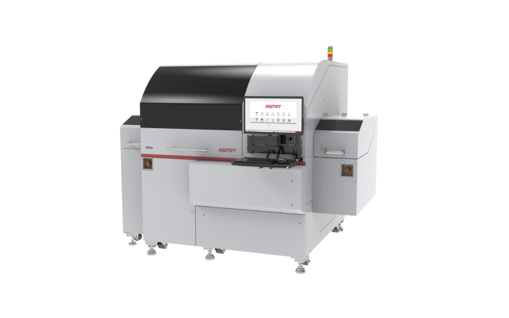
The multi-chip bonding solution MEGA combines epoxy dispensing and stamping with integrated 3D inspection and optional UV curing. Independently operating pick and bond arms with flip-pick and rotation units ensure precise alignment. Being highly configurable, MEGA meets the demands of advanced multi-chip packaging for optical transceivers, photonics, and sensor applications.
Dicing and grooving
The next-generation ALSI LASER1206 platform meets the growing demands of IDM and foundry manufacturers for wafer dicing and grooving, in advanced memory, logic, AI, and power applications. Its patented multi-beam UV laser technology enables high-precision processing with minimal thermal impact, reducing burr formation and preserving die strength. With support forfilm-framed and bare wafers,it has been validatedby multiple customers and leading plasma dicing suppliers.
SMDs and dies on a SMT production line
The award-winning SIPLACE CA2 combines high-speed die assembly directly from the wafer with SMT placement in a single platform. It processes SMDs via shuttle tables or conveyors as well as dies from sawn wafers in one operation, achieving throughput rates of up to 54,000 dies and 76,000 SMDs per hour with placement accuracy of up to ±10 µm @ 3σ.
“With advanced packaging and highly integrated SiP modules, the traditional boundaries between semiconductor manufacturing and SMT processes are increasingly blurring. ASMPT SMT Solutions offers platforms that extend the production spectrum to this next level,” says AnKyong Sung, General Manager for ASMPT SMT Solutions Korea.
SIPLACE TX micron is a placement platform developed for advanced packaging and high-density applications. Combining temperature-stable glass-ceramic scales, high-precision fiducial detection, high-resolution vision systems, and advanced vacuum tooling, it delivers placement accuracy of up to ±10 µm at throughput rates of up to 93,000 components per hour.