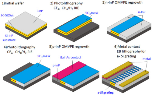
Belgian Research Centre along with the Ghent University has designed arrays of indium Phosphide lasers that has 300 mm silicon substrates in a CMOS line. This achievement will be providing a path towards a high volume and cost effective Photonic Integrated Circuits that will be taking this approach to data transfer speed between the logic and memory chips frequently. This when widespread will be adopted by the Silicon Photonics that as described by Hampered Says that This will be highly useful as one reason being the mismatch of the crystal lattice between the two types of materials. The partner of the research says that they have overcome the issue of mismatching between silicon and InP.
The partners used the high production grade epitaxial reactor to grow the InP selectively on the silicon designed in a pre template way. This formed an array of whole 300 mm substrate. This grating structure is responsible for providing the ideal performance for laser operations.


